In these tutorials of basic electronics, we will learn topics like BJT and MOSFET. They are the field-effect transistors and also the operational amplifiers in a short opamp, so first, we will complete the semiconductor materials before going to the diode.
The semiconductor materials are the backbone of electronics devices and circuits; that’s why it is crucial to know what are the different semiconductor materials available to us and also their properties.
The flow of charge through a cross-sectional area in the given time is called current. We have to check for the amount of current flowing through the material, and depending upon this current, we will categorize it into three categories.
- Conductor.
- Insulator
- Semiconductor.
Conductor
The term conductor is used for any material that will support a generous flow of charge when the voltage is applied across the terminals.
Copper and aluminum are the most commonly used conductors,
Insulator
An insulator is a material that offers very low conductivity when voltage is applied.
Let’s understand by example, mica and wood; the mica is very important in electrical industries. It is used for the thermal and electrical insulation in electrical and electronics equipment.
Semiconductor
A semiconductor is a material that has conductivity more than the insulators but less than the conductor.
Or we can say that the flow of current in a semiconductor is not as much as the conductor and not as low as the insulator; it is somewhere between the conductor and insulator.
The two most important semiconductor material is silicon and germanium, Si represents silicon, and GE represents germanium. We will see their properties below before that, let’s see the resistivity for the conductor insulator and semiconductor.
Resistivity
Resistivity is reciprocal for the conductivity, and the property of the material may vary material to material. Commonly represented by the Greek letter ρ, rho.
ρ = RA/l
Where: R is the electrical resistance, A is the area of cross-section, and “L” is the length of the wire.
The unit is an ohmmeter.
The resistivity for the conductor is 10^-6 ohm centimeter.
The resistivity for mica is 10^12-ohm centimeter. The amount of resistance this material is going to offer to the flow of charge is negligible for mica. In contrast, the resistivity of the silicon it is 50*10^3 ohm centimeter, and for germanium, it is 50-ohm centimeter.
The resistivity of a semiconductor is less than the resistivity of an insulator and higher than the resistivity of a conductor.
Let’s move to the next topic, that is the energy band diagram.
What is this energy band diagram?
When the atom is isolated with the nucleus having the neutrons, protons, and the orbits in which electrons are present, we call this orbits as L M N, as shown in the figure below.
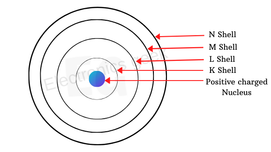
And the outermost orbit will have the valance electron because they will participate in the chemical reactions is a simple model for an isolated atom.
The electron is not isolated; it is present in the lattice in case of silicon the lattice in which the atom is present will form a particular structure. Thus the neighboring atom will influence this atom, as well as this atom will have some impact on the adjacent atoms because of the neighboring atoms. The outermost orbit will split into the valence band and the conduction band.
The electron present in the conduction band will participate in the conduction only if an electron present in the valence band move to the conduction band.
The only way to do that is to give this electron some energy. The amount of energy delivered to this electron must be equal to the gap, as shown in figure 1.2.
The energy gap is known as bandgap or forbidden bandgap. It called so because no electron is allowed in this region.
The energy band gap is represented as, Eg.
In the case of insulators, the energy bandgap is very large, hence the electron from the valence band requires more energy to go to the conduction band and participate in the conduction. That’s why they are not good conductors.
The bandgap is nearly equal to 6 electron volt for the insulators. As we know, one electron volt is equal to 1.6 * 10 ^19 joules, so we have to give 6 times more energy to make the electron appear in the conduction band.
For the semiconductors, the band is narrower, and the forbidden bandgap is nearly equal to 1 electron volt. For germanium, it is 0.75 electron volt, whereas, for silicon, it is equal to 1.6 electron volt.
You might be thinking why germanium has the lower energy band gap as compared to the silicon.
It is because of its atomic structure the number of orbits is more. Hence the force of attraction between the valence electron and the nucleus is smaller. In contrast, silicon has a lesser number of orbits. Therefore, the force of attraction is more strong on the electrons and needs more energy to fill.
It is like the nucleus is pulling the electron towards itself and need the energy to make this electron appear in the conduction band.
In Conductor the conduction band and the valence band is overlapping there is no forbidden bandgap. Thus the conductivity is very high because an electron is free to go from valence band to conduction band. It will participate in conduction without giving any extra energy to it; that’s why the conductivity is very high. as shown in the figure below.

Now let’s see the periodic table to have a better idea for the position of the germanium and silicon. In the periodic table, the elements are distributed depending upon the number of electrons in their outermost orbit. The germanium and silicon belongs to group 14
Why germanium and silicon belongs to group 14 ?
Because they have 4 atoms in the outermost orbit. As shown in figure 1.3
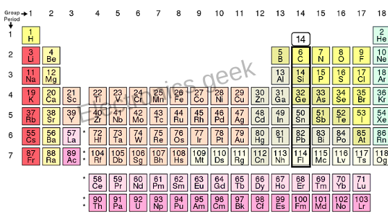
In the case of silicon, the total number of electron or the atomic number is 14. The maximum number of the electron in the first orbit equals 2, so we have two electrons in the first orbit, then we have 8 electrons. Hence, 2 + 8 is 10, and finally, we have 4 electrons in the outermost orbit, whereas in case of germanium, we have 32 electrons, 2 electrons in the first orbit, then 8, 18. Germanium also has 4 electrons in its outermost orbit; every element will have a stable state. For that, they must have a noble gas configuration. In the group of the noble gas, we have helium, neon, argon, Krypton, xenon, radon and the silicon.
The unique qualities of germanium and silicon are due to their atomic structure. The atoms of germanium and silicon form a definite pattern which continuously repeats itself, the one complete pattern known as crystal, and the periodic arrangement known as the lattice.
The lattice used in the diode and other electronic devices, so you have to keep this configuration in your mind. It will help you to understand intrinsic and extrinsic semiconductors.
So, In the next tutorial, we will study the intrinsic and extrinsic semiconductors as well as the electron and hole concept. And do check out the difference between BJT and FET.